
At the end of this lesson-
1. You will be able to explain Adder circuit.
2. You will be able to describe Half Adder circuit.
3. You will be able to describe Full Adder circuit.
4. You will be able to implement Full adder circuit using Half adder circuit.
5. You will be able to explain binary adder circuit.
Go for Bangla Version
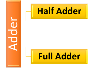
An adder is a combinational circuit or digital circuit in electronics that implements or performs addition of numbers. It is mainly designed for the addition of binary number, but they can be used in various other applications like binary code decimal, address decoding, table index calculation, etc. There are two types of Adder:
- Half adder
- Full adder
Half Adder Circuit
A half adder is a logical circuit that performs an addition operation on two binary digits. The half adder produces a sum and a carry value which are both binary digits.

Fig: Block Diagram of Half Adder
Half Adder can add two bits. So four different input sets or combination can be generated using two bits. Let’s see the truth table for four different input sets-

Fig: Truth table of Half Adder
From the truth table of the half adder we can see that the SUM (S) output is the result of the Exclusive-OR gate and the Carry(C) is the result of the AND gate. Then the Boolean expression for a half adder is as follows.
For the SUM bit:
SUM = A XOR B = A ⊕ B
For the CARRY bit:
CARRY = A AND B = A.B
Circuit of the half adder using Boolean function of SUM and CARRY-

Fig: Circuit of Half Adder
Logic circuit of Half Adder using only basic gates:
The following Boolean expression for sum(S) and carry(C) from truth table of half adder can be written according to SOP rules-

Circuit of Half Adder using above Boolean Expression-
 Fig: Circuit of Half Adder (Using Only Basic Gates)
- Implement the circuit of Half Adder using only NAND gate.
- Implement the circuit of Half Adder using only NOR gate.
Disadvantage of Half Adder
One major disadvantage of the Half Adder circuit when used as a binary adder, is that there is no provision for a “Carry-in” from the previous circuit when adding together multiple data bits.
For example, suppose we want to add together two 8-bit bytes of data, any resulting carry bit would need to be able to “ripple” or move across the bit patterns starting from the least significant bit (LSB). The most complicated operation the half adder can do is “1 + 1” but as the half adder has no carry input the resultant added value would be incorrect. One simple way to overcome this problem is to use a Full Adder type binary adder circuit.
Full Adder Circuit
The full adder is a logical circuit that performs an addition operation on three binary digits and just like the half adder, it also generates a carry out to the next addition column. Then a Carry-in is a possible carry from a less significant digit, while a Carry-out represents a carry to a more significant digit.
A full adder circuit is designed in such a manner that can take eight inputs together to create a byte-wide adder and cascade the carry bit from one adder to the another.
The main difference between the Full Adder and the previous Half Adder is that a full adder has three inputs. The same two single bit data inputs A and B as before plus an additional Carry-in (C-in) input to receive the carry from a previous stage as shown below.

Fig: Block Diagram of Full Adder
Full Adder can add three bits. So eight different input sets or combination can be generated using three bits. Let’s see the truth table for eight different input sets-

Fig: Truth table of Full Adder
The following Boolean expression for sum(S) and carry(Co) from truth table of Full adder can be written according to SOP rules-

Circuit of Full Adder using above Boolean Expression-

Fig: Circuit of Full Adder(Using Basic gates)
Let’s simplify above Boolean Expression of Full Adder-


Circuit of Full Adder using simplified expression of sum(S) and carry(Co)-

Fig: Circuit of Full Adder(Using Simplified expression)
- Implement the circuit of Full Adder using only NAND gate.
- Implement the circuit of Full Adder using only NOR gate.
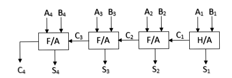
Implementation of Full Adder Circuit using Half Adder Circuit
We know,
For a Full Adder Circuit having three inputs like A, B and Ci and two outputs S and Co
S = AꚚBꚚCi
Co=(AꚚB).Ci + A.B
To implement the above Boolean expressions, two half adders and an OR gate are used in the following manner-

Fig: Implementation of Full Adder circuit using Half Adder circuit
For first Half Adder-
S1=AꚚB
C1=A.B
For second Half Adder-
S2=S1ꚚCi
C2=S1.Ci
Putting S1=AꚚB in the equation S2=S1ꚚCi , finally we got S2= AꚚBꚚCi ; which is the sum(S) of Full Adder.
Again, Putting the value of C1 and C2 in the equation Co=C1+C2, finally we got Co=(AꚚB).Ci + A.B; which is the carry(Co) of Full Adder.
So, It is possible to implement Full Adder Circuit using two Half Adder circuit and an OR gate.
Binary Adder:
A Binary Adder is a digital circuit that performs the arithmetic sum of two binary numbers provided with any length. Binary Adder are two types:
- Parallel Binary Adder
- Serial Binary Adder
Parallel Binary Adder: Parallel binary adders can add n-bits of two binary numbers in parallel. Parallel binary adder circuits can be created only with full-adders or half-adders and full-adders.
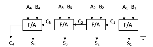
Example-1: Addition of 1101 and 1110 using binary adder circuit.
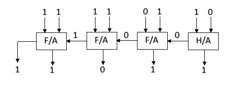
So, (1101)2 + (1110)2 = (11011)2
Example-2: Add 11011 and 10101 using binary adder circuit.
Example-3: Add 110 and 111 using binary adder circuit.
Serial Binary Adder
The serial binary adder or bit-serial adder is a digital circuit that performs binary addition bit by bit. The serial full adder has three single-bit inputs for the numbers to be added and the carry in. There are two single-bit outputs for the sum and carry out. The carry-in signal is the previously calculated carry-out signal. The addition is performed by adding each bit, lowest to highest, one per clock cycle.
Serial binary addition is done by a flip-flop and a full adder. The flip-flop takes the carry-out signal on each clock cycle and provides its value as the carry-in signal on the next clock cycle. After all of the bits of the input operands have arrived, all of the bits of the sum have come out of the sum output.
Lesson Evaluation-
Knowledge Based Questions:
a. What is Adder?
a. What is Half Adder?
a. What is Full Adder?
a. What is Binary Adder?
Comprehension Based Questions:
b. “Computer performs all arithmetic operations in a particular manner”-explain.
Creative Questions:
According to the block diagram answer the following questions:
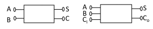
Block diagram-1 Block diagram-2
c) Implement the logic circuit of the block diagram-1 using only NAND gates.
d) Is it possible to implement the circuit of block diagram-2 using the circuit of block diagram-1? Analyze.
According to the figures answer the following questions:

c) Describe the adder circuit created using Fig-1 and Fig-2.
d) Analyze the role of two figures for creating adder circuit.
According to the figure answer the following questions:

c) Implement the circuit of the block diagram using basic gates.
d) Implement the circuit of new block diagram using only NOR gate after reducing one input.
Multiple Choice Questions:
1. Which of the following is used in addition?
a) Encoder b) Decoder c) Adder d) Counter
2. A 4-bit binary Adder to be created it needs –
i. four Full Adder
ii. three full Adder and one Half Adder
iii. three Half Adder and one Full Adder
Which one is correct?
a) i & ii b) i & iii c) ii & iii d) i, ii & iii
Written by,
- Mizanur Rahman (Mizan)
- Lecturer in ICT, Shaheed Bir Uttam Lt. Anwar Girls’ College , Dhaka Cantonment
- Founder & Author at www.edupointbd.com
- Software Engineer at mands IT
- Former Lecturer in ICT, Cambrian College, Dhaka
- Contact: 01724351470